
Why UV Sources Still Matter on the Fab Floor
Despite the rise of deep-UV lasers and high-power LEDs, many microfabrication steps still live or die by how uniformly, cleanly, and predictably we deliver ultraviolet photons over a wafer, panel, or roll-to-roll web. Photoresist exposure is the obvious case, but the list is much longer: surface activation for adhesion, low-temperature curing of hybrid polymers, UV-ozone cleaning before metallization, photochemical growth and removal steps in ALD/PEALD flows, and post-pattern hardening for thick negative resists. For these tasks, the source’s spectrum, irradiance stability, and field uniformity matter more than peak power alone. Electrodeless UV sources—plasmas sustained without electrodes by microwave or radio-frequency fields—have quietly become a strong option because they avoid electrode erosion, deliver broad and tunable emission, and scale to large, uniform fields with comparatively simple optics.
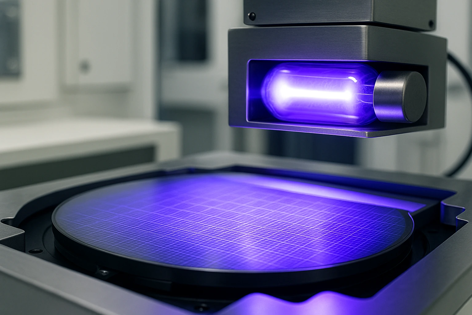
What “Electrodeless” Actually Means in Practice
In an electrodeless lamp, you create a UV-emitting plasma in a sealed bulb with no internal electrodes. Energy couples in from outside using microwave (typically 2.45 GHz) or RF fields through a dielectric envelope. The working gas can be mercury vapor, noble gases, halogens for excimer formation (Xe, Kr, Cl-based species), or metal halides. Because there are no electrodes inside, the chemistry of the plasma is cleaner and lifetime is not limited by cathode sputter or emissive coating fatigue. The envelope—often quartz or specialized silica—sets the short-wavelength cutoff and handles thermal load. The driver is a solid-state or magnetron-based source that ignites and sustains the plasma. The result is a bright UV emitter with high radiance, fast re-ignition, and the ability to run in geometries that are awkward for traditional lamps.
Electrodeless technology spans several families relevant to microfabrication: microwave-driven mercury lamps used for 254 nm and 185 nm lines; excimer lamps such as Xe2\*_2^\*2\* at ~172 nm for strong surface activation; KrCl at ~222 nm when far-UVC is desired; and broader-line metal-halide blends engineered for near-UV curing windows. Each family trades off penetration depth, ozone generation, and compatibility with optics and materials.
Spectral Engineering: Matching Photons to Processes
Microfabrication is sensitive to wavelength. SU-8 and similar epoxies respond strongly in the near UV, whereas UV-ozone cleaning and hydrophilization favor 185 nm photons that generate ozone in situ and break organic bonds. Electrodeless sources let you choose among discrete excimer lines or mercury lines without accepting electrode contamination or drift. Three spectral sweet spots dominate:
- 254 nm (Hg): Efficient for many photochemical reactions and useful for post-exposure bake assist and crosslinking in hybrid polymers when you want minimal ozone formation.
- 185 nm (Hg) + O2_22: Drives ozone formation and deep oxidation for organic removal and high-energy surface preparation; excellent for pre-metallization cleans at low temperature.
- 172 nm (Xe excimer): Extremely strong photon energy for breaking polymer chains and increasing surface energy; ideal for adhesion promotion on PTFE, PI, PET, and other stubborn substrates at room temperature.
Engineers increasingly deploy dual-band systems that combine a 172 nm plane source for rapid activation with a 254 nm flood for controlled curing, using shuttering or duty-cycle control to shape the dose recipe over time.
What’s New: Drivers, Geometry, and Uniformity
Recent advances have landed in three areas. First, solid-state RF and microwave drivers now regulate plasma power with tight feedback, flattening output drift and shortening warm-up, which reduces dose variability across a shift. Power supplies can modulate at kilohertz rates, enabling pulsed UV delivery that cuts thermal load while maintaining peak photochemistry.
Second, planar electrodeless lamps and microcavity plasma arrays have improved uniformity. Instead of a single bulb and heavy homogenizing optics, you can tile low-profile emitters behind a diffuser or integrate them close to the process plane, reducing cosine falloff and edge roll-off on large panels. For 200–450 mm wafers, this geometry eases the burden on fly’s-eye integrators and shortens working distance, improving irradiance with less power.
Third, materials and sealing have improved. Synthetic silica with low hydroxyl content lasts longer under 172 nm assault; getters and gas handling have reduced fill contamination; and thermally managed housings keep envelopes below devitrification thresholds. The practical outcome is extended lifetime at stable output, not just nameplate hours.
Metrics That Matter: How to Specify and Compare
A good electrodeless system spec translates directly into process confidence. The core metrics you should insist on are:
- Irradiance at plane (mW/cm²) at the working distance you will actually use, not at the source window.
- Uniformity across your field of view, with clear statistics (min/mean/max or ±% over a specified area).
- Spectral content with instrumented plots, including the fraction in target lines (172 nm, 185 nm, 254 nm) and any near-UV spill that might heat or cure unintended layers.
- Temporal stability after warm-up and under modulation, including short-term noise and long-term drift per hour and per 8-hour shift.
- Warm-up and re-ignition times, especially if your handler or robot relies on frequent shuttering.
- Lifetime under recipe conditions, not just at nominal power in open air; include decay-to-80% curves.
- Stray fields and EMC for RF/microwave systems, with shielding guidance for nearby measurement equipment and wafer charge protection.
- Ozone management rates (if 185 nm or 172 nm are involved), with exhaust and interlock recommendations.
When you compare to UV LEDs, remember that LEDs excel above ~255–265 nm with tight spectral width and easy digital control, but they cannot currently deliver high, uniform irradiance at 172–185 nm. Electrodeless sources bridge that gap and scale to larger areas more naturally, at the cost of ozone handling and RF/microwave plumbing.
Applications That Win Today on the Line
Electrodeless UV shines where you need strong surface chemistry at low temperature, large-area uniformity, or both.
- Surface activation for adhesion: 172 nm excimer flood tools raise surface energy on fluoropolymers and polyimides without plasma ion bombardment, avoiding roughening and preserving mechanical properties. The result is better metal lift-off and stronger bonding in flexible circuits and microfluidic laminations.
- UV-ozone cleans before deposition: A 185 nm + 254 nm combo removes organic residues and breaks adventitious carbon on oxide and nitride surfaces, improving contact resistance and adhesion with minimal thermal budget.
- Low-temperature curing and post-exposure hardening: For thick negative resists or hybrid dielectrics, controlled 254 nm exposure can tighten crosslink density without overbaking.
- Photochemical ALD and PEALD assist: UV during or between pulses can activate precursors at reduced temperatures, widening the process window for temperature-sensitive substrates.
- Maskless flood illumination for large panels: In display and sensor manufacturing, planar electrodeless lamps provide uniform fields over tens of centimeters, where point sources would demand burdensome optics.
- Polymer microstructure trimming: Short-wavelength exposure can depolymerize surface nanometers of photoresists, smoothing sidewalls or opening microfluidic vias with gentle, chemistry-driven removal rather than energetic ion etch.
In each case, the process win is a combination of chemical selectivity, thermal gentleness, and area scalability.
Integration, Safety, and Day-2 Realities
Integrating electrodeless UV is more about engineering discipline than exotic parts. You need proper RF shielding and cable management to protect metrology tools, ozone capture with interlocks, and thermal design so housings don’t drift optics or cook nearby adhesives. Dose control should rely on calibrated in-plane radiometry, not only power-supply readbacks. Because output depends on temperature and gas pressure inside the envelope, incorporate periodic field calibration with a traceable radiometer and bake that into the preventive maintenance schedule. For excimer systems, keep windows clean—172 nm is absorbed strongly by organic films, so a light, regular cleaning protocol pays back in stability.
Operator safety is straightforward: interlocked enclosures, UV-blocking viewports appropriate to the wavelength, and explicit ozone alarms where applicable. For far-UVC (around 222 nm), treat safety claims conservatively; in microfabrication, human exposure is both unnecessary and avoidable, so the right answer is robust shielding regardless of the emission line.
Choosing Between Electrodeless and Alternatives
If your process needs sub-200 nm photons or large, uniform flood fields, electrodeless sources earn a first look. If you require narrowband near-UV with pixel-level control, UV LEDs with optics or DMD/SLM projection may dominate. For highest-resolution lithography, lasers and steppers still rule. Many fabs now run a hybrid stack: LEDs for on-tool align and targeted curing above 260 nm, electrodeless excimer or mercury for activation/cleaning and broad flood, and lasers for precision steps. Thinking in terms of the dose budget—which photons at which steps—helps you place each source where it creates yield rather than complexity.
Where the Field Is Heading Next
The momentum is toward smarter drivers, thinner planar emitters, and closed-loop dose control at the process plane. Expect tighter integration with robot handlers and MES systems, faster on/off cycling that mimics LED convenience, and better modeling of photochemistry so recipes translate cleanly between tools and sites. As materials stacks in flexible and heterogeneous integration demand even lower thermal budgets, electrodeless 172–185 nm will remain valuable as a room-temperature chemistry engine.
With that landscape set—what electrodeless UV is, why its spectrum and geometry matter, and where it outperforms alternatives—the next step is to turn principles into practice by laying out concrete selection checklists, cost-of-ownership models, real-world recipes for activation and UV-ozone cleaning, and maintenance routines that keep irradiance inside tight control limits without overburdening the line, which is exactly where we pick up by unpacking dose mapping methods, field-uniformity tuning tricks, and a comparative playbook for 172 nm versus 185/254 nm stacks so that process engineers can make confident choices without pausing production.
Dose Mapping at the Process Plane
The quickest way to turn theory into yield is to measure dose where it matters—at the substrate. Start with a calibrated radiometer that covers your target wavelength and dynamic range; place it at the working distance and scan a grid across the exposure field. Record irradiance and compute dose with the planned recipe timing. If the sensor footprint is larger than your finest features, augment with photochromic film or resist-dose wedges that integrate spatial nuance. Build a “heat map” of min/mean/max values, then translate it into actionable knobs: lamp height, diffuser position, and driver power. Repeat the map after 30, 60, and 120 minutes of continuous operation to capture thermal drift, and again after any maintenance that might shift alignment. Dose mapping is not a one-time qualification—fold it into monthly preventive maintenance and after any lamp swap so that process windows track reality rather than assumptions.
Field Uniformity Tuning Without Exotic Optics
Uniformity lives and dies on geometry. Small changes in standoff distance often smooth hot spots because inverse-square gradients relax with height; a few millimeters can cut ±5% variation in half at modest cost to peak irradiance. Diffusers help, but choose materials with known transmission at 172–254 nm and watch for yellowing under dose. For planar emitters, slight angular cant—one or two degrees—can cancel symmetry-driven bright bands. If you must use a single-bulb source, pair it with an integrating light pipe or a multi-lens fly’s-eye homogenizer sized to the field; align so that the source image sits slightly out of focus at the substrate to discourage Moiré with patterned layers. Finally, eliminate parasitic reflections: matte-black baffles and non-fluorescent coatings around the exposure bay prevent ghost illumination that confounds maps and inflates local dose.
Recipe Playbook: Activation, UV-Ozone, and Post-Exposure
For 172 nm activation on polymers, a typical sequence begins with 10–60 seconds at 50–200 mW/cm², nitrogen purge optional for materials that dislike ozone. Watch contact angle as your acceptance metric; stop when you reach the plateau (often 10–20° for fluoropolymers) to avoid over-embrittlement. For UV-ozone cleaning using 185 + 254 nm, run oxygen-rich ambient with controlled exhaust. Start with 2–5 minutes at 20–60 mW/cm² 254 nm plus at least a few mW/cm² 185 nm; verify with XPS or contact resistance. Increase time rather than power if you see residue re-deposition or film stress. For post-exposure hardening of thick negative resists, detune to 254 nm only and step the dose in short bursts (e.g., 5×30 seconds with 30–60 seconds cool between) to limit thermal creep while tightening crosslink density. Document every recipe with the accompanying dose map so technicians can catch drift by eye: if a clouded diffuser or aging envelope shifts brightness patterns, your uniformity plot will betray it before yield does.
Selecting 172 vs 185/254: A Comparative Checklist
Choose 172 nm when surface activation is the goal, especially for low-temperature adhesion on PTFE, PI, PET, or fluorinated dielectrics. Expect dramatic contact-angle drops and strong functionalization with minimal ion damage. Plan for ozone management even if you purge, because 172 nm interacts with residual oxygen and organics on hardware. Choose 185/254 nm for cleaning oxide and nitride surfaces, breaking adventitious carbon, and promoting metal adhesion without roughening. The 185 nm line drives ozone formation efficiently; 254 nm sustains oxidation and photolysis. If your stack is sensitive to ozone (e.g., some silver inks or organometallic layers), lean toward controlled 254 nm or shield interim layers. When throughput and area dominate, planar electrodeless 172 nm arrays simplify uniformity over large panels; when selectivity matters and you can tolerate modest field sizes, bulb-plus-integrator 185/254 rigs remain cost-effective and robust.
Cost of Ownership and Throughput Reality
Electrodeless systems win when they replace slow plasma cleans or high-temperature bakes with minutes of room-temperature photon work. Factor the full cost: lamp or envelope lifetime to 80% output under your recipe, driver efficiency, scheduled cleaning of windows and diffusers, and downtime for calibration. Ozone handling adds ducting, sensors, and periodic filter replacement; RF shielding adds enclosure and ground work. On the credit side, you gain faster cycle times, lower scrap from thermal warpage, and fewer consumables than wet cleans. A rough rule: if your UV step displaces more than five minutes of oven or plasma time per lot, the payback period is often under a year once uniformity and stability are locked in. Keep a simple KPI dashboard—dose stability (±%), uniformity (±%), uptime (%), contact angle or contamination metric—so finance and production see the same truth operators do.
Stability, Calibration, and Control Loops
Because electrodeless output depends on the plasma’s internal pressure and temperature, open-loop power readouts are not enough. Close the loop at the plane: a reference photodiode or radiometer behind a UV-transparent witness window can serve as a surrogate if it is correlated to in-plane dose. Better, embed a brief calibration pulse in each run—before wafers arrive—measuring a standard patch on a process dummy. Use that to nudge driver power so in-plane irradiance lands on target despite warm-up or ambient shifts. Track long-term decay with control charts and set automatic maintenance triggers at, say, 90% of nominal dose at constant power. When you swap envelopes or drivers, re-map and re-establish the correlation curve rather than assuming the old coefficients still apply. This discipline prevents quiet drift from becoming a yield event.
Integrating With Tools, Robots, and MES
Modern drivers support fast digital modulation; exploit it. Program settle-and-expose sequences that start only after irradiance is within tolerance, and interlock exposure to chuck vacuum and door status. If your handler parks substrates under the lamp for non-productive seconds, use low-duty pre-glow rather than full power to keep the plasma stable without building dose. Log recipe parameters, in-plane dose, and uniformity indices to MES with lot IDs so later root-cause investigations have data, not memories. For multi-lane exposure on large panels, synchronize lamp segments to motion stages: overlapping, time-weighted illumination can smooth stitch lines that otherwise etch into photoresist as faint bands.
Safety and Facilities: Make It Boring
A UV tool that is exciting is a UV tool you will one day regret. Keep it boring with interlocked doors, wavelength-appropriate viewing panels, and signage. Treat far-UVC claims conservatively; your operators never need direct exposure to 222 nm or 254 nm to run a good process. Ozone alarms and airflow monitors belong inside the interlock chain; if exhaust falls below the specified flow, exposure should not start. RF hygiene is usually straightforward: braided grounds, EMI gaskets on doors, and filtered feed-throughs. Walk the bay with a spectrum meter during qualification—if your AFM, ellipsometer, or probe station acts up, add shielding now, not after a failure analysis blames intermittent RF.
Troubleshooting by Symptom
If edges under-cure while the center is fine, raise standoff distance or enlarge the diffuser; check for vignetted optics or a warped diffuser frame. If dose drifts upward during long runs, suspect thermal stabilization—improve housing cooling or insert brief idle periods. If contact angle plateaus too high after 172 nm activation, increase time rather than power, or purge with dry air to limit by-products that passivate the surface. If residual carbon persists after UV-ozone, verify that 185 nm flux is present; many tools inadvertently filter it out with silica windows or aged coatings. If camera-based alignment fails during exposure, RF leakage may be modulating sensors—add local shielding or move cables away from lamp fields. Keep a one-page playbook at the tool listing these symptoms and the two or three most likely fixes.
Extending to Advanced Flows
Once the basics are stable, fold electrodeless UV deeper into the line. Pair 172 nm activation with silane adhesion promoters in microfluidics; use staged UV-ozone before PVD to lower contact resistance in via chains; add a gentle 254 nm post-pattern step to harden high-aspect SU-8 prior to electroforming. In heterogeneous integration, pre-bond cleaning at 185/254 nm can improve polymer-to-oxide bonds at temperatures that would otherwise relax alignment. For PEALD, interleave low-dose UV to activate inert surfaces between precursor pulses, widening the process window without resorting to harsher plasmas. The rule is the same: measure dose, map uniformity, and translate materials responses into short recipe snippets that fit tact times without dominating them.
Looking Forward With Practical Optimism
The direction of travel is clear: thinner planar emitters, smarter drivers, and tighter plane-side feedback. Expect vendors to ship tools with built-in dose cameras that see what your wafer sees, and software that optimizes segment timing automatically. But the fundamentals won’t change: uniformity depends on geometry, stability depends on calibration, and yield depends on aligning photons with chemistry. If you make dose mapping routine, keep recipes modest and repeatable, and let a handful of well-chosen metrics police drift, electrodeless UV becomes a boring, reliable engine for adhesion, cleaning, and curing—a quiet enabler of fast cycles and cool temperatures in a world that increasingly demands both.